

1. Introduction: The Shift to Vertical Integration in Semiconductors
As semiconductor devices become increasingly compact and powerful, the industry is witnessing a revolutionary transformation in how chips are designed and packaged. At the forefront of this transformation is 3D semiconductor packaging a technology that enables higher performance, reduced latency, better thermal management, and smaller form factors. This report explores key concepts, applications, materials, trends, and market leaders driving this evolution.
Invest in Our Premium Strategic Solution: https://www.towardspackaging.com/download-sample/5275
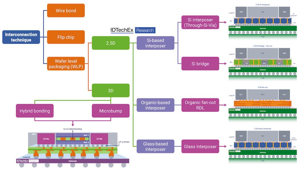
2. Understanding the Architecture: 2.5D vs. 3D Packaging
The distinction between 2.5D and 3D semiconductor packaging is fundamental for understanding the technology’s trajectory.
-
2.5D Packaging: Combines multiple chips (dies) on a silicon interposer. The interposer enables high-density interconnects and efficient communication among chips without stacking them vertically.
-
3D Packaging: Involves chip stacking—one die placed on top of another—and uses Through-Silicon Vias (TSVs) to enable direct vertical connections between dies. This reduces the interconnect length, boosting speed and power efficiency.
Both approaches enhance system performance but cater to different cost, complexity, and thermal management requirements.
If there’s anything you’d like to ask, feel free to get in touch with us @ sales@towardspackaging.com
3. High-Performance Applications: Powering the Next Generation
3D packaging is critical in applications that demand compact, high-performance computing power:
-
AI and Machine Learning Chips: These chips require high memory bandwidth and low-latency interconnects—perfect use cases for TSV-based 3D integration.
-
Internet of Things (IoT): Devices need to be compact and energy-efficient. 3D packaging helps integrate multiple functionalities in a limited footprint.
-
Smartphones and Consumer Electronics: The push for smaller yet more powerful devices demands stacking solutions that offer both miniaturization and performance.
-
Automotive Systems: As vehicles evolve with autonomous features and high-speed computing, thermal reliability and real-time data processing become critical—domains where 3D packaging excels.
4. Performance Edge: Thermal and Electrical Advantages
The architecture of 3D packaging delivers:
-
Improved Thermal Dissipation: With optimized heat sinks and power distribution, the design reduces thermal hotspots, crucial for AI and edge computing workloads.
-
Shorter Signal Paths: TSVs significantly reduce signal travel distance, resulting in faster communication and lower power consumption.
-
Greater Functionality in Smaller Footprints: Enables chip designers to pack more into smaller packages—ideal for edge devices, wearables, and high-end processors.
5. Material Matters: The Building Blocks of 3D Integration
Advanced materials are vital in ensuring package integrity, reliability, and electrical performance:
-
Substrates: High-density interconnect substrates provide mechanical support and electrical routing.
-
Adhesives and Underfill Materials: Used to protect and bind stacked dies, managing stress and improving thermal conductivity.
-
Molding Compounds: Ensure durability, protect against moisture and contamination, and improve heat resistance.
Material innovation is crucial in enabling finer line widths, better heat dissipation, and higher integration densities.
6. Driving Miniaturization: Bandwidth, Size, and Speed
3D packaging directly enables:
-
High Bandwidth Memory (HBM): Especially in GPUs and AI accelerators, where high-speed data access is vital.
-
Compact Architectures: Reduces board size, ideal for mobile and IoT devices.
-
Power Efficiency: Lower interconnect lengths and optimized thermal paths reduce overall power consumption, meeting environmental and performance goals.
7. Innovation Frontiers: FOWLP and Chiplet Architecture
The market is not just about vertical stacking—it’s evolving rapidly with innovations like:
-
Fan-Out Wafer-Level Packaging (FOWLP): Offers improved electrical performance and slimmer form factors. Eliminates the need for substrates, allowing thinner, lighter packages.
-
Chiplet-Based Designs: Breaks monolithic chips into smaller, functional units (chiplets), which are interconnected using advanced packaging. This approach reduces cost and improves flexibility in chip design.
Both technologies are pivotal in scaling beyond Moore’s Law, offering flexibility and efficiency in high-end computing.
8. Industry Leaders: Key Companies Shaping the Market
Several global players are dominating and innovating within the 3D semiconductor packaging space:
-
ASE Technology: A pioneer in advanced packaging, offering both 2.5D/3D integration and FOWLP solutions.
-
Amkor Technology: Known for scalable high-volume production of 3D and wafer-level packages, especially in mobile and automotive applications.
-
TSMC: Not just a foundry giant, TSMC leads with 3D Fabric technologies like CoWoS® and InFO®, vital for AI and high-performance computing.
-
Intel: Driving chiplet and Foveros 3D stacking technologies, especially for data center and client CPUs.
-
JCET Group: Offers a full suite of advanced packaging, including SiP and 3D ICs for consumer electronics and automotive markets.
9. Strategic Implications for Manufacturers and Suppliers
The evolution of 3D packaging presents strategic growth avenues for component suppliers, material innovators, and assembly specialists:
-
Opportunities in High-Density Substrates and TSV Manufacturing
-
Material Innovation for heat management and interconnect insulation
-
Collaboration with Fabless Companies to create customized 3D ICs
-
Sustainability Solutions for greener packaging processes and materials
10. Conclusion: Building Tomorrow’s Electronics Today
3D semiconductor packaging is more than a trend—it’s a critical enabler of the next technological leap. For manufacturers across the value chain, from materials to assembly and testing, aligning with this shift is essential to remaining competitive.
📢 Are you ready to position your company at the forefront of next-gen semiconductor packaging? Connect with us today to explore partnership and innovation opportunities.
Source: https://www.towardspackaging.com/insights/3d-semiconductor-packaging-market-sizing
Get the latest insights on packaging industry segmentation with our Annual Membership – https://www.towardspackaging.com/get-an-annual-membership
About Us
Towards Packaging is a leading global consulting firm specializing in providing comprehensive and strategic research solutions. With a highly skilled and experienced consultant team, we offer a wide range of services designed to empower businesses with valuable insights and actionable recommendations. We stay abreast of the latest industry trends and emerging markets to provide our clients with an unrivalled understanding of their respective sectors. We adhere to rigorous research methodologies, combining primary and secondary research to ensure accuracy and reliability. Our data-driven approach and advanced analytics enable us to unearth actionable insights and make informed recommendations. We are committed to delivering excellence in all our endeavours. Our dedication to quality and continuous improvement has earned us the trust and loyalty of clients worldwide.
Browse our Brand-New Journal:
Towards Healthcare: https://www.towardshealthcare.com
Towards Automotive: https://www.towardsautomotive.com
For Latest Update Follow Us: https://www.linkedin.com/company/towards-packaging/
Get Our Freshly Printed Chronicle: https://www.packagingwebwire.com/